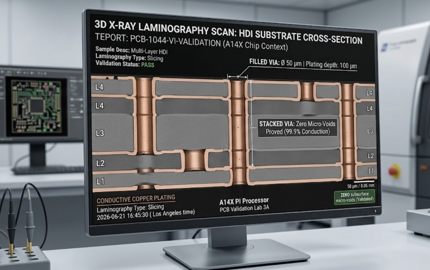
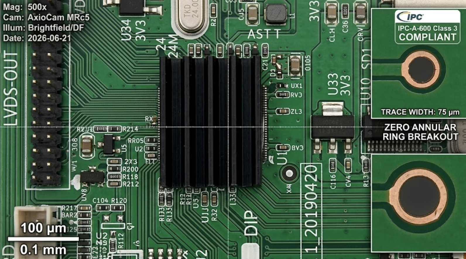
Shenzhen, Guangdong Oct 11, 2026 (Issuewire.com) - Smart wearables have evolved rapidly over recent years. Advanced wristwear now performs complex biomedical tracking alongside wireless communication. This technological shift changes the physical demands placed on electronic circuit boards. Traditional printed circuit board assembly handles consumer electronics with relaxed spacing tolerances. However, modern wearable devices require micro-scale density and complex geometry. Engineers face severe space limitations because compact enclosures must house display modules, sensors, and batteries simultaneously. Consequently, electronics manufacturing requires a highly specialized approach to guarantee long-term field reliability. Selecting a certified Reliable Panel Smart Bracelet PCBA Supplier (https://www.aozite-pcba.com/smart-bracelet-pcba-oem-manufacturing-product/) represents a fundamental step for technology hardware developers who seek to eliminate early product failures. To govern this delicate manufacturing landscape, the electronics industry relies on IPC-A-600 guidelines. This globally recognized standard dictates the structural acceptability of printed boards before component placement begins. 1. Micro-Registration vs. Standard Clearance: IPC-A-600 Standards for Fine-Pitch Conductor Alignment Traditional consumer electronic products usually feature circuit trace widths exceeding 150 micrometers. This relatively large dimension provides circuit board fabricators with a comfortable margin for internal layer registration. In contrast, smart wearable technology compresses trace spacing to thresholds below 75 micrometers. These dense trace networks are necessary to accommodate high-density components such as 0.35-millimeter-pitch wafer-level packages and tiny 01005 passive parts. IPC-A-600 Chapter 2 deeply regulates these conductor characteristics, focusing on micro-registration accuracy. Under standard industrial criteria, small conductor nicks or minor annular ring breakouts are often acceptable if minimum lateral spaces remain. However, the high-precision requirements of smart bracelet panels alter these allowances completely. High-density designs demand target conditions where zero annular ring breakout occurs on component lands. Furthermore, trace width variations must remain under 10 percent to protect high-frequency signals. Even microscopic misalignments can disrupt impedance matching on critical Bluetooth or Wi-Fi communication lines. To prevent these localized failures, specialized manufacturing facilities must utilize advanced technologies. For instance, Shenzhen Aozite Technology Co.,Limited addresses these challenges through the deployment of sub-micron Laser Direct Imaging systems. These advanced exposure machines ensure exact trace registration, while high-resolution solder mask inspection tools verify alignment before components pass through the reflow oven. 2. The Margin of Error at the Perimeter: Board Edge Clearance Limitations and Bezel Constraints Traditional circuit board layouts maintain a standard clearance buffer of 0.5 millimeters or more between internal copper traces and the routed board edge. This wide border shields the active circuitry from mechanical stresses during panel routing and final assembly singulation. However, smart bracelet panels operate under extreme volumetric restrictions. To maximize display space and battery volume inside sleek bezels, designers position ground planes within 0.2 millimeters of the physical board edge. IPC-A-600 Chapter 1.2 establishes strict parameters for board edge conditions, specifically targeting defects like haloing, delamination, and edge burrs. Standard electronic assemblies frequently overlook localized micro-fractures or structural haloing penetrating up to 50 percent of the distance to the nearest conductor. In high-precision smart wearables, this lenient approach introduces severe vulnerability. Because wrist-worn devices experience constant exposure to human sweat and ambient moisture, any edge defect creates a direct pathway for contaminants. Moisture penetrates the compromised fiberglass layers, generating latent galvanic corrosion that eventually causes catastrophic short circuits. Therefore, industrial manufacturers require pristine, burr-free edges where haloing is virtually non-existent. This precise care ensures that structural barriers protect internal circuits throughout the operational lifespan of the wearable device. 3. Sub-Surface Integrity: Blind and Buried Via Plating Quality in HDI Wearable Architectures Most standard electronic devices rely on simple multilayer architectures connected by traditional through-hole vias. These vertical channels run completely through the circuit board, presenting straightforward plating challenges for manufacturing facilities. In comparison, high-density smart wristwear requires High-Density Interconnect architectures featuring stacked blind and buried vias. These micro-vias connect specific internal layers without penetrating the entire board substrate. This feature allows engineers to route complex signal pathways across eight or more layers within a thin 0.8-millimeter profile. IPC-A-600 Chapter 3.3 sets forth rigorous acceptability criteria for internal substrate features, emphasizing via fill completeness and copper wrap plating thickness. Standard assembly lines focus primarily on basic copper continuity within through-hole barrels, tolerating small internal voids in non-functional fill areas. However, high-performance wearable fabrication allows no such compromise. Stacked blind vias require complete, void-free filling with copper or conductive epoxy paste, followed by a flat copper cap plating. If internal micro-voids remain inside a stacked via structure, they transform into dangerous thermal traps. During subsequent double-sided surface mount reflow cycles, the trapped air expands rapidly under intense heat. This localized thermal expansion shears the fragile internal micro-via connections, creating intermittent open circuits that defy standard testing methods. To mitigate this underground risk, Aozite OST PCBA (https://www.aozite-pcba.com/about-us/) (Shenzhen Aozite Technology Co., Limited) integrates multi-dimensional inspection protocols into its core quality management workflow. The inspection team utilizes high-precision 3D X-ray laminography to analyze internal copper structures, catching subsurface voiding before boards advance to final product assembly. 4. Preventing Latent Thermal Failures: Inner Layer Delamination and Voiding Tolerances Wearable electronics experience unique environmental and mechanical stresses that differ vastly from stationary consumer hardware. A desktop appliance remains stationary in a controlled room. Conversely, a smart bracelet faces continuous mechanical flexing, physical impacts, and human body heat. These external variables demand superior structural integrity to prevent inner-layer delamination over extended operational lifetimes. IPC-A-600 Chapter 3.1 explicitly outlines the boundaries for laminate voids, resin recession, and layer separation under rigorous thermal stress testing. Standard electronic items operating under Class 2 guidelines permit small internal material voids, provided the defects do not bridge adjacent circuit patterns. Smart wearable panels, by contrast, must adhere to stringent criteria that align with Class 3 industrial electronics. Microscopic voids that appear harmless in a standard device will expand rapidly when subjected to the repeated thermal cycling of wearable operation. This internal separation breaks internal signal traces and disrupts performance. To achieve the required baseline durability, engineering groups often transfer rigorous manufacturing standards from other highly demanding electronic fields. For example, applying techniques developed for one-stop PCBA turnkey solutions for medical electronics and health equipment (https://www.aozite-pcba.com/application/one-stop-pcba-turnkey-solution-for-medical-electronics-and-health-equipment/) ensures that consumer wearable substrates possess identical structural resilience. This cross-industry quality standard involves comprehensive thermal shock pre-screening, which exposes bare boards to extreme temperature swings before component placement. This proactive methodology eliminates latent delamination risks, guaranteeing that the underlying substrate handles the thermal and mechanical realities of everyday user wear. 5. The Aozite OST PCBA Execution Matrix: Translating IPC Guidelines into High-Yield Turnkey Reality Translating the strict requirements of IPC-A-600 into an efficient, high-yield manufacturing process requires massive infrastructure and deep engineering expertise. Aozite OST PCBA bridges the gap between theoretical quality standards and practical volume execution through a structured, data-driven production matrix. The process begins during the early stages of product development, where the engineering team performs exhaustive Design for Manufacturing reviews on client engineering files. Specialists analyze Gerber layouts to optimize pad geometries, conductor widths, and layer stack-ups against IPC target conditions, fixing potential fabrication faults before physical manufacturing starts. On the production floor, the facility deploys extensive automated machinery optimized for sensitive, ultra-thin substrates. The operation utilizes eight advanced, high-speed surface mount technology lines that feature automated paste printing inspectors, high-accuracy component placers, and multi-zone reflow ovens. This automated infrastructure handles complex rigid-flex boards without causing mechanical warping or layer separation. Following assembly, every panel undergoes a comprehensive validation loop. The factory combines automated optical inspection, flying probe diagnostics, and dedicated functional testing to ensure absolute quality. This verification loop confirms that every shipped board aligns perfectly with international quality benchmarks. Sourcing Quality at the Fabrication Stage High assembly yields and long-term field reliability for smart wearable devices are not achieved by chance; they are engineered at the bare-board level. By choosing an experienced production partner that aligns its processes with IPC-A-600 criteria, hardware innovators can scale up their product lines smoothly. True manufacturing success relies on deep engineering discipline and meticulous quality verification rather than superficial visual checks. Hardware brands maximize their market success when they select an assembly partner capable of executing these precise micro-scale standards consistently. For detailed inquiries regarding high-precision fabrication capabilities or to request a comprehensive engineering file evaluation, technology developers can connect directly with the specialized engineering teams via the official enterprise portal: https://www.aozite-pcba.com/.
Media Contact
Aozite OST PCBA *****@aozite-pcba.com http://www.aozite-pcba.com/